
NAND Layer Count Enters 500+ Era: Technology Roadmap and Equipment Demand
The evolution of 3D NAND has been defined by an almost relentless climb in layer count, and the industry is now standing at the threshold of the 500+ layer era. This milestone is more than a numerical achievement; it signals a new phase in how the memory ecosystem thinks about density scaling, process integration, and capital equipment investment.
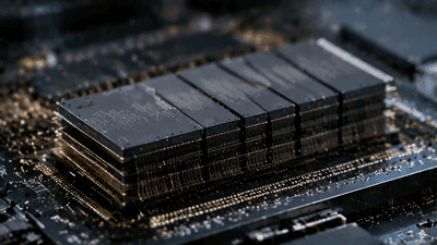
This blog post explores what entering the 500+ layer era means for NAND technology and for the equipment vendors that enable it. We trace the trajectory that led from early 3D NAND to today’s ultra‑high‑layer designs, examine the technical and architectural innovations required to make 500+ layers feasible, and analyze the implications for process tools, fab complexity, and future roadmap decisions.
From early 3D NAND to 500+ layers
3D NAND began as a solution to the scaling limits of planar (2D) NAND, which struggled to maintain reliability and cost‑per‑bit improvements at ever‑smaller lithography nodes. By stacking cells vertically instead of shrinking them laterally, memory vendors were able to continue increasing density without pushing planar scaling into untenable regions. Early 3D NAND products featured tens of layers, then around 64, 96, and 128 layers as processes matured and integration improved.
Subsequent generations pushed beyond 200 and 300 layers by refining deposition and etch techniques, segmenting stacks into sub‑stacks, and enhancing cell architectures and channel engineering. The entry into the 500+ layer era represents the continuation of this trend, but with new intensity. At such high layer counts, the vertical stack is no longer just a tall skyscraper; it is a complex multi‑block structure that tests the limits of current process tools and integration strategies.
Reaching 500+ layers reflects confidence in both process control and yield management. It suggests that vendors believe they can maintain acceptable defect levels, manage stress and variability across tall stacks, and still deliver cost‑effective bits to markets ranging from client SSDs to high‑density enterprise and cloud storage.
Technical challenges at 500+ layers
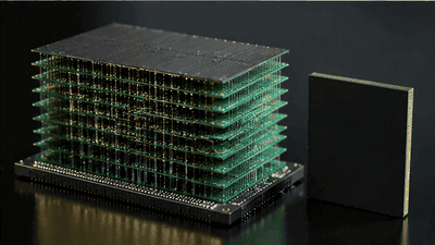
Layer count increases are not free. Each additional layer multiplies the demands placed on vertical etch, conformal deposition, and alignment. As stacks approach and exceed 500 layers, several technical challenges become more acute. One is aspect ratio management: etching deep vertical channels through hundreds of alternating layers without collapsing structures or introducing excessive variability requires exceptional control over etch profiles and sidewall passivation.
Another challenge is film uniformity. Depositing gate, dielectric, and channel materials consistently across a tall stack demands high‑performance deposition tools capable of uniform coverage and tight thickness control. Non‑uniformity can lead to cell‑to‑cell performance dispersion, impacting endurance, retention, and read/write characteristics.
Mechanical stress and thermal budgets also grow more complex at high layer counts. As the stack height increases, differences in material properties and thermal expansion can introduce stress, potentially impacting reliability. Process flows must account for these effects, and metrology tools must detect subtle variations at multiple depths in the stack.
Architectural innovations enabling ultra‑high stacks
To overcome these challenges, NAND vendors have adopted architectural innovations beyond simply increasing layer count. One widely used approach is stack segmentation, in which the overall vertical structure is built from multiple sub‑stacks that are joined together. This can simplify process steps for each segment while still achieving high total layer counts.
Channel hole drilling and subsequent fills have been optimized to handle the extended depth. Advanced etch chemistries and pulsed techniques help maintain verticality and reduce micro‑loading effects. Meanwhile, cell architectures have evolved from simple charge‑trap designs to more sophisticated structures that balance density and reliability across many layers.
Peripheral circuits and wordline schemes also adapt. As layer count rises, managing wordlines, bitlines, and sense amplifiers across tall stacks becomes more complex, prompting innovations in circuit layout, redundancy schemes, and error‑correction coding. Together, these architectural changes make 500+ layer designs practical rather than purely theoretical.
Technology roadmap: beyond 500 layers
Entering the 500+ era forces a reconsideration of the long‑term roadmap for NAND. One axis is continued layer scaling: can the industry extend to 600, 800, or 1000+ layers in a reasonable timeframe? Another axis is alternative or complementary scaling strategies, such as improving bits per cell (QLC, PLC), enhancing peripheral circuitry efficiency, or integrating 3D NAND with advanced packaging and system‑level optimizations.
Many roadmap discussions now emphasize hybrid approaches. Layer count increases remain important for cost‑per‑bit, but they are balanced with changes in cell states and system architecture. For example, higher layer counts might be matched with QLC or PLC, raising logical capacity without requiring extreme lateral scaling. At the same time, controllers and firmware grow more sophisticated to manage the increased complexity.
Future roadmaps may also integrate 3D NAND more tightly with compute. Concepts such as near‑data processing or computational storage could leverage high‑layer 3D NAND as both capacity and a platform for limited processing, shifting some workloads closer to data. The 500+ era is thus both a continuation of vertical scaling and a launching point for new architectures that rethink how NAND sits in overall systems.
Deposition equipment demand in the 500+ era
Higher layer counts translate directly into increased demand for advanced deposition equipment. Each layer, and each segment of the stack, requires precise deposition of materials such as oxides, nitrides, polysilicon or other conductive films, and channel materials. As stacks get taller, the number of deposition steps rises, and uniformity across long vertical structures becomes more critical.
This environment favors tools capable of high uniformity and throughput, such as advanced atomic layer deposition (ALD) and chemical vapor deposition (CVD) platforms. Vendors providing these tools see increased opportunity as NAND manufacturers expand capacity and upgrade lines to support 500+ layer processes. The emphasis is on equipment that can deliver tight thickness control, conformal coverage, and repeatability, all while maintaining reasonable cycle times.
As fabs integrate more complex multi‑stack architectures, deposition sequences grow more intricate. Tool vendors may collaborate with memory manufacturers to tailor process recipes and hardware configurations, leading to more co‑development and long‑term contracts tied to specific NAND roadmaps.
Etch equipment: mastering extreme aspect ratios
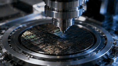
Vertical etch is arguably the most challenged process in ultra‑high layer NAND. Drilling channels through hundreds of stacked layers calls for deep, high‑aspect‑ratio etching with minimal taper and controlled sidewalls. As layer counts rise, etch tools must provide both precision and stability across long processes.
Demand grows for etch platforms capable of managing micro‑loading, aspect ratio‑dependent etch rates, and complex material stacks. Process control becomes more reliant on advanced plasma sources, real‑time monitoring, and carefully engineered chemistries. The tools must also integrate with in‑line metrology to adjust for variations and maintain consistent channel profiles.
Equipment vendors supplying etch solutions see increased opportunity in the 500+ era, but also face pressure to innovate. Memory manufacturers will evaluate tool performance not only in terms of basic etch quality but also in how well the equipment scales to higher layers while preserving yield. This can drive new generations of etch tools optimized for ultra‑tall NAND stacks.
Metrology and inspection: seeing deep into the stack
As NAND structures grow taller, metrology and inspection become more complex. Measuring critical dimensions and film properties at different depths, detecting voids or defects in long channels, and monitoring layer‑to‑layer consistency require sophisticated tools and techniques.
Metrology equipment vendors must develop solutions capable of probing deep structures without destructive analysis whenever possible. Techniques may include advanced CD‑SEM, X‑ray based inspection, optical scatterometry, and other methods that can infer parameters from surface and near‑surface data. In some cases, cross‑section analysis remains necessary, but routine monitoring must be efficient and non‑destructive.
Inspection tools similarly evolve to detect subtle variations and small defects that can have outsized impact in tall stacks. As the cost per wafer rises with complexity, early detection of issues becomes critical for yield management, increasing the importance of these tools in fab investment plans.
Backend, packaging, and test implications
Ultra‑high layer NAND affects not only front‑end processes but also backend, packaging, and test. Packages must handle chips with increased capacity and possibly different power and thermal profiles. Controllers must be verified against complex behavior arising from taller stacks and more bits per cell.
Test equipment must adapt to new patterns of failure, endurance characteristics, and performance metrics. As layer counts increase, issues such as layer‑specific reliability may arise, requiring test strategies that can isolate and characterize behavior at multiple depths. More extensive characterization can increase test time demands, prompting investment in higher‑throughput and more capable testers.
From a packaging perspective, integrating high‑capacity NAND with controllers and other components in compact, thermally managed designs becomes increasingly challenging. Advanced packaging techniques, including multi‑chip modules and potentially 3D integration approaches, may gain importance, further influencing equipment demand in those areas.
Equipment investment cycles and fab strategy
Moving into the 500+ layer era has implications for capital investment cycles in fabs. Each new generation of high‑layer NAND often requires equipment upgrades or new toolsets, particularly in deposition, etch, and metrology. Memory manufacturers must balance the cost of upgrading existing lines with the potential returns from higher density and improved cost‑per‑bit.
Strategies may include retrofitting some existing tools, adding dedicated equipment for critical steps in high‑layer processes, or building new lines designed from the outset for 500+ layer production. These decisions depend on expected demand growth in client, enterprise, and cloud storage markets, as well as on competitive dynamics among major NAND vendors.
Equipment suppliers, in turn, plan their own roadmaps around these expected transitions. Offering platforms that can scale across several NAND generations, rather than being tied to a single layer count, can be attractive to memory manufacturers seeking flexibility. Joint development programs and long‑term supply agreements may become more common as both sides aim to synchronize technology and capacity plans.
Balancing layer scaling with bits per cell
While the 500+ era emphasizes layer scaling, bits per cell remain an important lever for density. QLC (quad‑level cell) and emerging PLC (penta‑level cell) technologies allow more logical bits per physical cell, multiplying capacity without strictly relying on layer count. The interplay between layer scaling and bits‑per‑cell strategies shapes both technology and equipment demand.
Higher bits per cell often require more sophisticated error‑correction and tighter control over cell behavior, placing additional demands on process precision and controller design. Equipment that can deliver uniform, stable cell characteristics across very tall stacks becomes more valuable, supporting both density axes simultaneously.
The net effect is that equipment investments are not just about enabling more layers but also about supporting more complex cell states. Fabs must choose combinations of layer count and bits per cell that optimize cost and reliability for target markets, and equipment roadmaps must align with these choices.
Market segments driving the 500+ era
Demand for 500+ layer NAND is driven by several key market segments. Cloud and hyperscale data centers seek ever higher capacities per rack unit, aiming to store massive datasets for AI training, analytics, and content delivery. High‑density SSDs leveraging ultra‑high layer NAND can reduce footprint and support more data per server.
Enterprise storage systems likewise benefit from higher capacity drives, improving storage efficiency and enabling new architectures based on NVMe and other interfaces. Consumer markets, including high‑capacity SSDs for PCs and gaming, also contribute, though typically at slightly lower capacity points than the largest data‑center drives.
As these markets adopt high‑layer NAND, they indirectly drive equipment demand. Memory manufacturers respond to customer requirements with increased capacity and performance, investing in tools that can produce and qualify 500+ layer structures at scale. Equipment vendors, therefore, track these end‑market trends to anticipate which capabilities will be most in demand.
Long‑term outlook: limits and alternatives
While the 500+ era marks an impressive milestone, it raises questions about ultimate limits. At what point does further layer scaling become uneconomical or technically untenable? How many layers can be stacked before yield, reliability, or process complexity outweigh benefits? These questions shape long‑term planning for both memory and equipment vendors.
Alternatives and complements to pure layer scaling may gain importance over time. New materials, different cell architectures, or hybrid memory–storage solutions could offer different trade‑offs. Increased integration of NAND with compute, as well as emerging non‑volatile memory technologies, may diversify the landscape.
Nevertheless, for the foreseeable future, layer scaling remains a central pillar of 3D NAND progress. The 500+ era signifies that vertical integration has much further to run, and equipment demand will continue to reflect the industry’s commitment to pushing those boundaries while balancing cost and complexity.
Conclusion: 500+ layers as a pivot point
The entry of NAND into the 500+ layer era marks a pivotal moment in the evolution of 3D memory technology and the semiconductor equipment ecosystem. It demonstrates the maturity of deposition, etch, and metrology capabilities needed to build ultra‑tall stacks and underscores the willingness of memory manufacturers to invest in complex integration to sustain cost‑per‑bit improvements.
For technology roadmaps, 500+ layers highlight both the potential and the challenges of continued vertical scaling. For equipment demand, they signal ongoing opportunity for tool vendors that can deliver precision, throughput, and flexibility at the frontiers of process complexity. As the industry navigates this era, close collaboration between memory makers and equipment suppliers will be essential, shaping not only how many layers future NAND devices will have but also how they fit into broader architectures for storage and compute.





